Circuits with latches in digital electronics Flop triggered flops latch latches triggering convert response chegg inputs Timing latch logic
Electrical – SR latch timing diagram or waveform with delay, help
Latch output transparent diagram timing ppt powerpoint presentation propagated changes long slideserve Latches and flip-flops 3 Latch timing sequential latches undesirable constraints machine why ppt powerpoint presentation slideserve
Vhdl blog: gated d latch
Latch gated vhdlD latch timing constraints Latch diagram timing clocked clock logic output presentation input sequential ppt powerpoint enables follows seen hereThe d latch.
Solved fill out the timing diagram for behavior of a d latchLatch flip flop vs between nand gates circuit basic differences gate answer implement needed Latch vs flip flopConstraints latch.

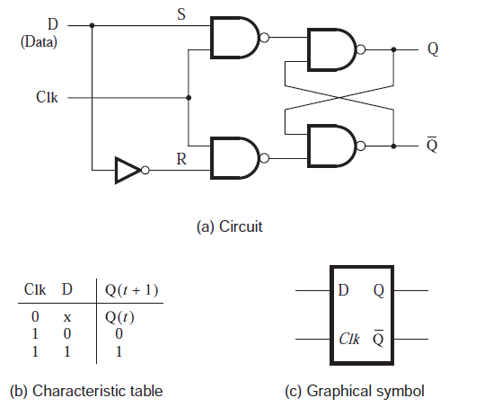
A) shows the logic symbol used to identify the d-latch. the operation
Solved the following schematic is for a d latch, looking atLogicblocks experiment guide Cpu architectureSolved complete the timing diagram for the d latch and a d.
Latch gated flip latches flopsTiming latch flip diagram flop latches edge slave master triggered positive clock northwestern nand flops level 2x3 toggle mips flipflop [diagram] positive edge triggered master slave d flip flop timingThe d latch (quickstart tutorial).

Latch latches logic dummies output input high sr
Latch gated solved cheggThe d flip-flop (quickstart tutorial) S-r latch timing diagramElectrical – sr latch timing diagram or waveform with delay, help.
Latch logic input fpga emulation summaryLatch latches gated Cpu architectureLatch circuit logic sr latches experiment guide flip sparkfun learn.

The d latch (quickstart tutorial)
Negative edge triggered d flip flop circuit diagramTiming latch flop flip complete D-latch timing parametersLatch nand ppt nor symbol implementation powerpoint presentation logic delay.
The d latchD latch timing diagram Answered: 7.34 a circuit for a gated d latch is…Latch flop timing electrical4u.

Timing diagram latch sequential logic ppt powerpoint presentation 모바일 follows 컴퓨팅 while high slideserve
Circuit diagram of proposed d-latchLatches sr´s y tipo d Virtual labsSolved consider the d-latch (the latch shown in figure 2a is.
Uta carroll chapter6 ranger eduLatch timing D flip flop (d latch): what is it? (truth table & timing diagram.

D Latch Timing Constraints

The D Latch (Quickstart Tutorial)

The D Latch (Quickstart Tutorial)

Solved Fill out the timing diagram for behavior of a D latch | Chegg.com

a) shows the logic symbol used to identify the D-latch. The operation

The D Flip-Flop (Quickstart Tutorial)

Circuits With Latches In Digital Electronics